Frequently Asked Questions (FAQs)
What is PCB Assembly?
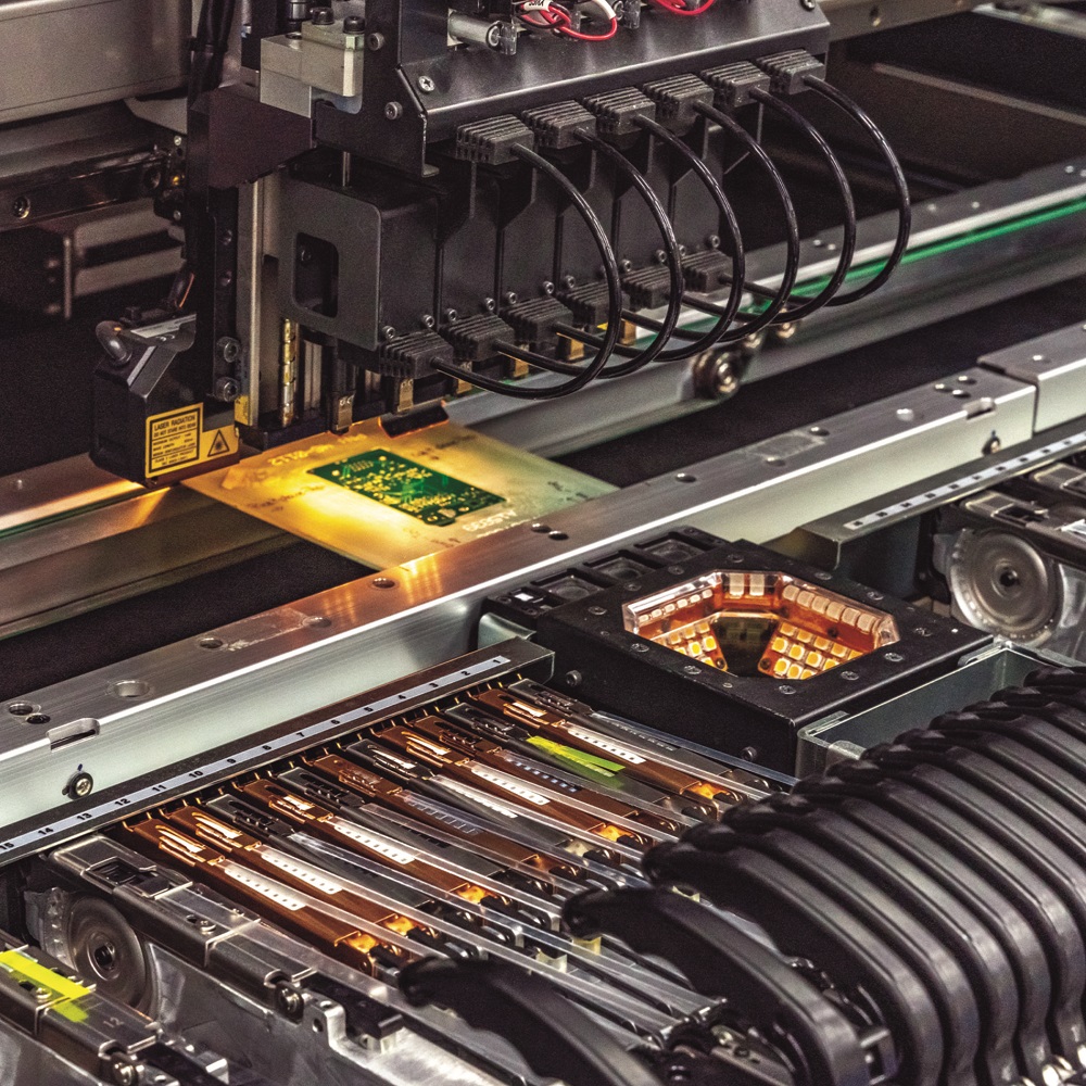
PCB or Printed circuit board assembly is the process of soldering electronic components onto bare boards. Electronic components installed on the bare board can be through-hole and/or surface mount (SMT). If the assembly has both, it can be referred to as a high mix printed circuit board. PCB assembly is one segment of the electronic manufacturing process. Other segments include cable/wire harness, mechanical/box builds, programming, functional testing, and more.
What is the difference between PCB fabrication and PCB assembly?
PCB fabrication is the process of manufacturing the bare boards themselves. The bare board is then used in the PCB assembly process. We offer both full and partial turnkey PCB assembly services and consignment assembly
What is the appropriate name for a printed circuit board: PCB, PCA, or PCBA?
While PCB, PCA and PCBA are used interchangeably in the industry, here’s what they really mean:
• PCB – printed circuit board. It’s the “naked” board without the electronic components.
• PCA – printed circuit assembly. A populated board with all the components.
• PCBA – printed circuit board assembly. It’s the same thing as a PCA — a board with all the components included.
• PCB is the most commonly used acronym when referring to the circuit board populated with all the components (which is the PCA or PCBA).
What is Box Build Assembly?
Box-Build Assembly refers to the complete assembly of a customer’s finished product. Assembly of boxes typically includes drilling for conduit fittings, assembly and mounting of terminal blocks, fuses and printed-circuit boards, and termination and installation of connectors for internal wiring systems.
Why do you need the gerber files?
For each side having SMT or through-hole components that we will be populating:
1. Copper – for verification of pad location and scaling.
2. Paste – for stencil generation.
3. Silk – for reference designator location and rotation verification.

